
A Breakthrough in Nano-Circuit Transfer Technology
A groundbreaking technology has been developed that enables the transfer of metal circuits floating on water directly onto any desired surface. This innovation, created by a South Korean research team, allows for the precise placement of ultra-fine nanocircuits onto plant leaves, fruits, curved automotive surfaces, and robot exteriors without causing any damage. The potential applications of this technology span multiple industries, including smart agriculture, wearable health care, and bioelectronics.
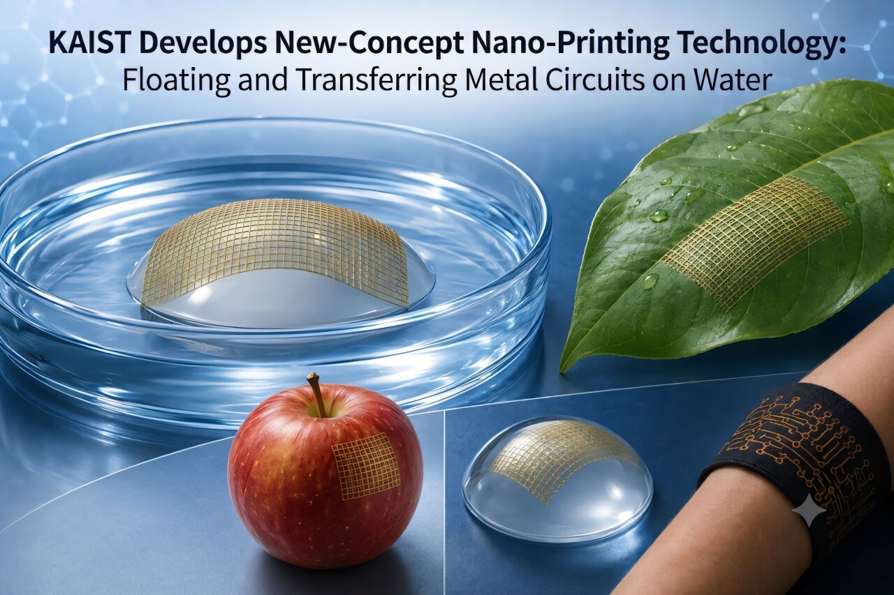
A New Approach to Nano-Transfer Printing
A joint research team led by Distinguished Professor Inkyu Park from the Department of Mechanical Engineering, Dr. Jun-Ho Jeong from the Korea Institute of Machinery and Materials, and Professor Junseong Ahn from Korea University has successfully developed water-floating nano-transfer printing (WF-nTP). This innovative method enables precision metal thin films floating on water to be transferred to 3D surfaces. The study was published in Nature Communications.
Conventional nano-transfer printing (nTP), which is widely used to manufacture electronic devices and sensors, typically requires high heat, intense pressure, adhesives, or toxic chemical solvents. As a result, applying this method to biological tissues or complex curved surfaces that are sensitive to heat and pressure has proven highly challenging.
To overcome these limitations, the research team proposed a completely new approach: floating metal circuits on the surface of water.
How the Technology Works
The team deposited an ultra-thin layer of metals such as gold (Au), platinum (Pt), palladium (Pd), or nickel (Ni) onto a polymer mold. They then used plasma gas, a high-energy state of ionized gas, to selectively remove (etch) part of the mold. When this structure is placed in water, water infiltrates through the microscopic gaps, causing the 20-nanometer (nm) thick metal film to float to the surface on its own while perfectly maintaining its original shape.
The research team transferred the metal circuits using a “scooping” method, which involves submerging the target object beneath the floating film and slowly lifting it upward. As the water evaporates, capillary force (the force that moves liquid through narrow spaces) tightly adheres the circuit to the surface. Once the water completely dries, intermolecular forces come into play, securing the circuit firmly in place without the need for any adhesive.
Expanding the Possibilities
Notably, the team also succeeded in transferring circuits onto hydrophobic (water-repellent) surfaces, such as lotus leaves. By adding a small amount of ethanol to the water to lower its surface tension (the property of a liquid surface that causes it to shrink), they effectively overcame a major limitation of conventional technologies.
This technology holds strong potential for widespread application because it can adapt to diverse surfaces while preserving the nano-patterns. Using this method, the research team fabricated surface-enhanced Raman scattering (SERS) sensors, which are used for highly sensitive detection of trace chemical substances, and attached them directly to plant leaves and fruit surfaces.
With this, they successfully detected thiram, a pesticide component, on the surfaces of leaves and fruits. Furthermore, they implemented a wearable, high-performance hydrogen gas sensor by transferring a palladium (Pd) mesh onto highly flexible thermoplastic polyurethane (TPU) fibers.
Future Implications
Prof. Park said, “This technology is highly significant as it shatters the substrate limitations of conventional nano-transfer printing, allowing nano-patterns to be transferred onto sensitive surfaces like living plant leaves or human skin without heat or adhesives. We expect it to evolve into a core platform technology for wearable sensors and bioelectronics, finding applications in smart agriculture for pesticide detection without damaging crops, wearable health monitoring devices, bioelectronic devices, and electronic skins for next-generation robots.”
Key Applications
- Smart Agriculture: Detecting pesticides on plant leaves and fruits.
- Wearable Health Care: Developing high-performance sensors for health monitoring.
- Bioelectronics: Creating devices that interface with biological systems.
- Robotics: Enhancing robot exteriors with electronic skins.
This technology represents a significant advancement in the field of nanotechnology and opens up new possibilities for the integration of electronic components into a wide range of surfaces and environments.